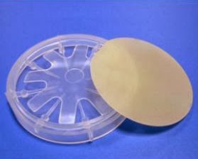
PAM-XIAMEN, a leading GaN substrate manufacturer, offer GaN substrates and
its relative wafers. GaN substrate is used in UV or blue
Laser Diodes for next generation DVDs, high brightness LEDs for general
lighting and high power, high frequency transistors for cellular phone base
stations and photovoltaic applications.We continued to develop new GaN substrates such as
large-diameter c-plane substrates as well as nonpolar/semipolar GaN substrates.
In particular, we overcame the green gap problem and developed true green laser
diodes by selecting an optimal crystal plane. And now we give a brief
troduction of GaN substrate as follows:
| C plane, n type GaN substrate: 2”, 1”, |
| C plane, semi-insulating GaN substrate: 2”, 1”, |
| A plane, n type GaN substrate |
| M plane, n type GaN substrate |
| 1)15mm,10mm,5mm ",1.5",2"Free-standing GaN substrate |
| Orientation:C-axis(0001)+/-0.5° |
| Conduction Type:N-type |
| Size:(50.8)+/-1mm |
| Thickness:260+/-20um |
| Primary Flat Location:(1-100)+/-0.5° |
| Primary Flat Length:16+/-1mm |
| Primary Flat Location:(1-100)+/-0.5° |
| Secondary Flat Length:6+/-1mm |
| Dislocation Density:<5x106cm-2 |
| Marco Defect Density:A grade<=2cm-2 |
| Resistivity(300K):<0.5Ω·cm |
| TTV:<=15um |
| BOW:<=20um |
| Surface Finish:Front Surface:Ra<0.2nm.Epi-ready polished C plane, semi-insulating GaN substrate |
| 2)15mm,10mm,5mm ",1.5",2"Free-standing GaN substrate | |||||||||||
| Orientation:C-axis(0001)+/-0.5° | |||||||||||
| Conduction Type:Semi-insulating | |||||||||||
| Size:230+/-20um(280+/-20um) | |||||||||||
| Thickness:260+/-20um | |||||||||||
| Dislocation Density:<5x106cm-2 | |||||||||||
| Marco Defect Density:0cm-2 | |||||||||||
| Resistivity(300K):>106Ω·cm | |||||||||||
| TTV:<=15um | |||||||||||
| BOW:<=20um | |||||||||||
Surface Finish:Front Surface:Ra<0.2nm.Epi-ready polished
|
| And also provide for: |
A plane, n type GaN substrate
M plane, n type GaN substrate
GaN on sapphire
GaN substrate market:
Near- and long-term market applications for bulk GaN substrates are
examined, along with motivations and challenges for adopting the substrate
technology for specific device applications. The near-term demand for bulk GaN
is driven primarily by laser diodes, while solid state lighting and power
electronics will drive the long-term demand. Challenges to achieving broad
market penetration include increased volume production and reduced
manufacturing cost, which are needed to penetrate incumbent GaN device
technologies based on foreign substrates.
If you find them interesting, please visit us: www.qualitymaterial.net or contact with us: gan@powerwaywafer.com.
| Related
Products: gan template blue/green/red GaN gan substrate growth gan substrate sumitomo gan substrate led gan substrates progress status |
If you find them interesting, please visit us: www.qualitymaterial.net or contact with us: gan@powerwaywafer.com.
* Export license needed.

Is it possible to use 4” non-patterned sapphire for fabrication?
ReplyDeleteNot possible, currently all the manufacturers swift to patterned sapphire based wafer, including us, however if you really need flat sapphire based wafer, we we can offer 2" size.
DeleteA fine quality educational blog! I like the way blogger presented information regarding the concerned subject. Thanks for posting such a nice blog.
ReplyDeletesapphire wafer